NPU Chip Design & Verification — CNN Accelerator (Tape-out)
Silicon-validatedNPU 流片项目 — CNN 推理加速器
22 nm CNN inference NPU, pre-silicon verification ownership through tape-out and silicon validation.
- Role
- Team-developed; personal ownership: pre-silicon verification
- Dates
- Feb 2026 – present
- Verif
- AI
- RTL
- NPU
One-line hook: collaborative 22nm CNN inference NPU; took a LeNet-style network through RTL → tape-out → silicon validation; personal ownership on pre-silicon verification (UVM env, scoreboard, coverage closure, CDC sign-off).
Role
- Project type: collaborative chip development with industry mentors
- Network: CNN inference (LeNet-style, MNIST / CIFAR-10 class)
- Personal ownership: pre-silicon verification — UVM environment, scoreboard with bit-accurate reference models, coverage closure, CDC sign-off across 4 async clocks
- Design contributions: reviewed and co-developed selected modules (FP16 MAC datapath, AXI/APB/SPI bus integration, clock-mux / reset-sync paths)
Tech Stack
SystemVerilog · UVM · Synopsys VCS / Verdi · AXI VIP · SPI agent · RAL (SPI→APB adapter) · CDC sign-off · coverage-driven verification · Python regression harness
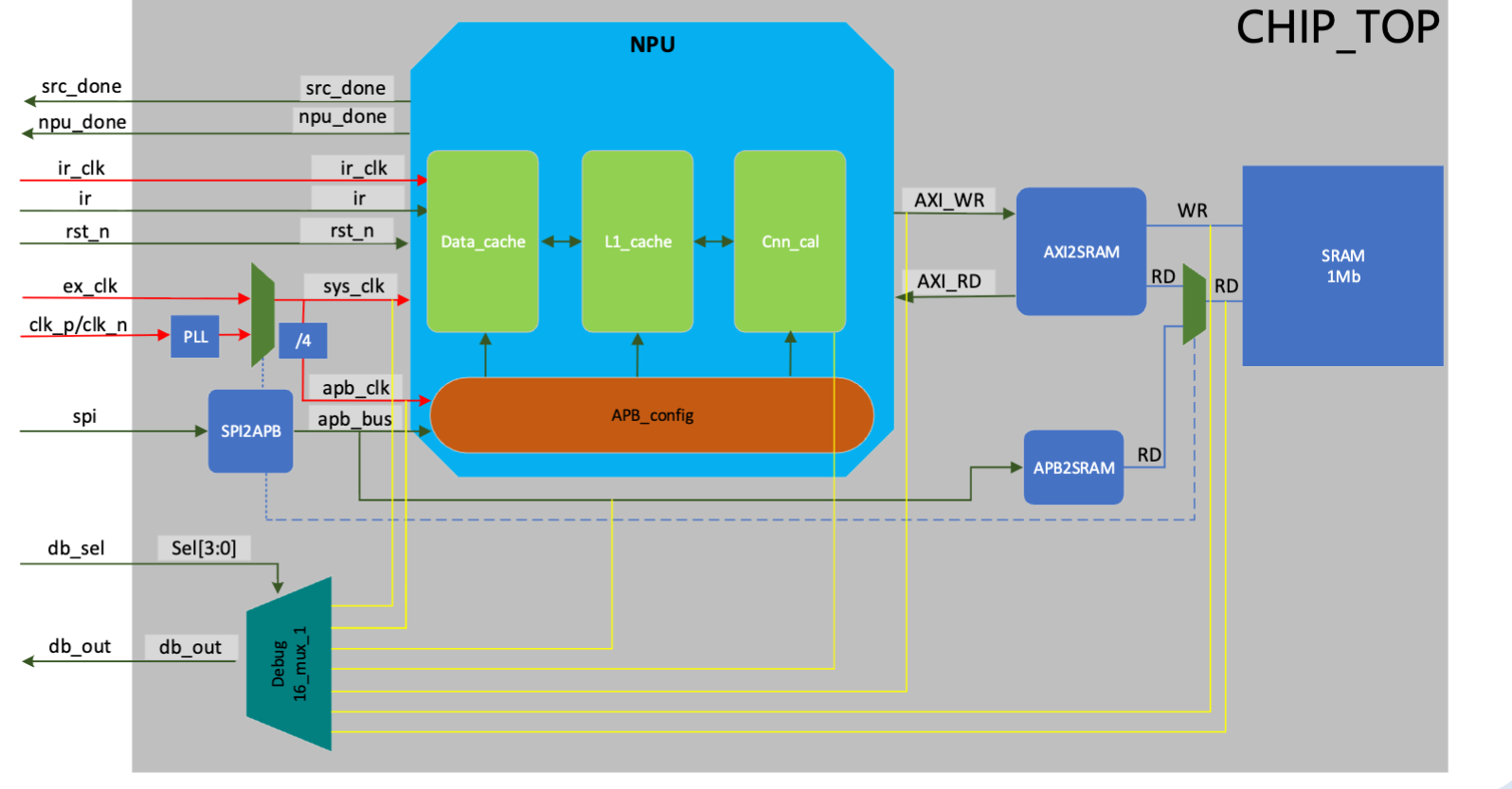
Architecture (simplified)
CNN inference datapath:
Image (INT8) → AXI ingest → Cache
→ INT8 → FP16 dequant
→ Conv (multi-channel MAC + add-tree)
→ ReLU
→ MaxPool 2×2
→ Conv → ReLU → MaxPool
→ FC → ReLU → FC → MaxResult (classification)
→ AXI write-out
Bus stack: AXI for data movement (image / weight / output), APB for register configuration, SPI for debug access (spi2apb bridge). 4 asynchronous clock domains with sync_bit + async FIFO crossings.
Verification Highlights
- Built full-chip UVM environment on Synopsys AXI/SPI VIP with a custom image UVC (RGB raster stimulus) and RAL via SPI→APB register adapter.
- Authored vplan + UVM sequences for register read/write, MNIST/CIFAR-10 golden inference, multi-frame switching, SPI SRAM readback, and PLL bring-up.
- Built bit-true scoreboard against an SW golden model covering FP16 dequant, multi-channel MAC, max-pool, and 3-stage FC.
- Closed CDC sign-off across 4 async clocks; ran VCS/Verdi regression and coverage via a Python harness with
mem_loadbackdoor.
Status (2026-05)
- Silicon back from fabrication, validated by a separate post-silicon team.
- Pre-silicon verification deliverables (UVM env, vplan, scoreboard, coverage closure) signed off prior to tape-out.
English STAR (interview-ready)
Short (15 s)
Co-developed a 22 nm CNN inference NPU with industry mentors and led the pre-silicon verification, taking the design from RTL through tape-out. Built the full-chip UVM environment, the bit-true scoreboard, and closed CDC sign-off across four async clocks. Silicon came back validated.
Medium (45 s)
The project was a collaborative chip-development effort with industry mentors. The chip is a 22 nm CNN inference NPU targeting LeNet-style networks on MNIST and CIFAR-10 — an FP16 datapath fed by an INT8 frontend, with an AXI/APB/SPI bus stack and four asynchronous clock domains. My personal ownership was pre-silicon verification. I built the full-chip UVM environment on top of Synopsys AXI and SPI VIP, added a custom image UVC for RGB raster stimulus, and wrote the RAL with a SPI-to-APB register adapter. I authored the vplan and sequences for register read/write, golden-inference flows, multi-frame switching, SPI SRAM readback, and PLL bring-up. I built a bit-true scoreboard against an SW golden model covering the FP16 dequant, multi-channel MAC, max-pool, and three-stage FC. I closed CDC sign-off across all four async clocks and managed VCS/Verdi regression and coverage with a Python harness using a memory-load backdoor. The silicon came back validated.
Long (90 s — adds design-side context)
The chip is a 22 nm CNN inference NPU built collaboratively with industry mentors. The network is LeNet-style for MNIST and CIFAR-10: two convolution stages with multi-channel MAC plus add-tree, ReLU activations, 2×2 max-pooling, two fully-connected layers, and a classification head. Data flows from an INT8 image through an AXI ingest path, a dequant to FP16, then through the convolution / pooling / FC pipeline, and out over AXI. Bus stack is AXI for data movement, APB for register configuration, SPI for debug access via a
spi2apbbridge. Four asynchronous clock domains, crossed withsync_bitand async FIFOs. I owned pre-silicon verification end-to-end: built the full-chip UVM environment on Synopsys AXI / SPI VIP, added a custom image UVC, and wired RAL via a SPI-to-APB adapter. The vplan covered register R/W, MNIST and CIFAR-10 golden inference, multi-frame switching, SPI SRAM readback, and PLL bring-up. The scoreboard was bit-true against an SW golden model across FP16 dequant, multi-channel MAC, max-pool, and the FC stages. I closed CDC across all four clocks. On the design side I reviewed and co-developed selected blocks — the FP16 MAC datapath, the AXI/APB/SPI integration, and the clock-mux / reset-sync paths — and reviewed RTL for clock-mux behavior, reset synchronization, and PLL bring-up. The silicon came back validated by a separate post-silicon team.
Interview defense — “Is this a course / which company?”
This project is intentionally framed as collaborative chip development with industry mentors alongside the master’s program — not a sole-authored course project, not an internship deliverable I can name. Architecture-level decisions were led by experienced industry engineers; my personal ownership is the pre-silicon verification side. The specific company / foundry / customer is not disclosed in public materials; happy to elaborate offline under NDA-appropriate context.